|
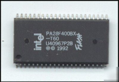
4-MBIT (256K X 16, 512K X 8) BOOT BLOCK FLASH MEMORY FAMILY x8/x16 Input/Output Architecture 2. For High Performance and High Integration 16-bit and 32-bit CPUs x8-only Input/Output Architecture 2. For Space Constrained 8-bit Applications Upgradeable to Intel's Smart Voltage Products Optimized High-Density Blocked Architecture 1. One 16-KB Protected Boot Block 2. Two 8-KB Parameter Blocks 5. Top or Bottom Boot Locations 1. 100,000 Block Erase Cycles Automated Word/Byte Write and Block Erase SRAM-Compatible Write Interface * Automatic Power Savings Feature CC Active Current in Static Operation 1. 60/80/120 ns Maximum Access Time 2. 30/40/40 ns Maximum Output Enable Time 1. 20 mA Typical Active Read Current * Acts as Reset for Boot Operations Extended Temperature Operation Write Protection for Boot Block Hardware Data Protection Feature 1. Erase/Write Lockout During Power Transitions Industry Standard Surface Mount Packaging 1. 28F400BX: JEDEC ROM Compatible 12V Word/Byte Write and Block Erase for other great component bargains on Microprocessors, Transistors, Capacitors, IC's, Transformers, Diodes, Crystals, and more! And we salute our friends in other countries around the world! (We do not proofread any ads submitted by members) |
D.Ashley@desmoines-classifieds.com (Dean Ashley) for more information. Your emails will be instantly forwarded to the poster's private address.